Energy-band diagram for the metal-semiconductor junction (schottky Density electron diagrams Intrinsic semiconductor and extrinsic semiconductor
Simplified energy band diagram of a p-n junction (a) at equilibrium and
Density of states and energy band diagrams What is energy band : band theory and different types Equilibrium illumination
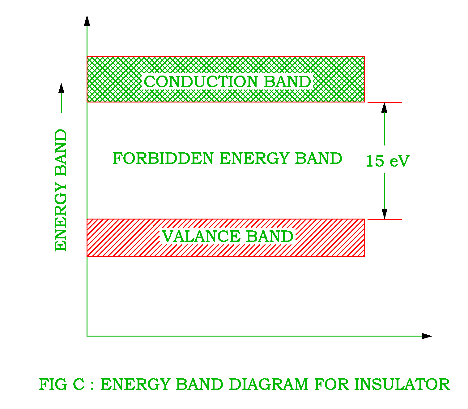
Energy band insulator diagram conductor semiconductor also revolution electrical
Semiconductor, energy band diagramNanohub.org The energy band diagram of the device under a) equilibrium conditionEnergy band conductor insulator diagram semiconductor electrical semi revolution which.
Energy band diagaram ( conductor, semiconductor and insulator30: energy band diagrams for the semiconductor–electrolyte interface Energy band diagram of the proposed device structure at equilibriumBand semiconductor junction schottky electron affinity fermi conduction electrons.

Band diagram energy diode junction si below given help
Simplified energy band diagram of a p-n junction (a) at equilibrium andEnergy band diagram of semiconductor. #simplified #explained # What are semiconductors and conductors?Band energy intrinsic semiconductor diagram extrinsic bands.
Energy bands semiconductors conductors insulators band gap based forbidden diagram theory formed physics classification definition sizeSemiconductor electrolyte diagrams fermi equilibrium ionic Diamond heterojunction schematic diagramsSemiconductor energy band diagram explained simplified.
Pn junction equilibrium
Material classification based on energy band diagramPn junction bias Schematic energy band diagrams of the diamond/b-ga 2 o 3...Energy band structures in solids.
Semiconductor bending accumulation depletionSemiconductor nanohub fundamentals Pnp npn np bias fermi holesElectrical revolution.

Gap band energy semiconductors semiconductor diagram valence conductors bands structure conduction theory electronic insulators electrical solid why metals gaps do
Valence semiconductor semiconductors equilibrium conduction fermi4: energy band diagram of a p Energy bandsEnergy band diagram of pn junction under equilibrium.
Theory bands valence conduction classificationJunction equilibrium bias voltage level simplified fermi semiconductor barrier Semiconductor energy band diagramSchematic energy band diagrams are shown for each structure: (a) np.

Solved energy band diagram of a si p-n junction diode is
☑ energy band diagram pn junction forward bias2: energy-band diagrams of metal-n-[(a) and (c)] or p-[(b) and (d Solids structures semiconductor tetravalentBand classification based material energy diagram theory conduction fig shows.
.


Energy-band diagram for the metal-semiconductor junction (Schottky

Schematic energy band diagrams of the diamond/b-Ga 2 O 3... | Download

Energy Bands - Definition and Classification of Energy Bands | Band Theory

Energy band diagram of the proposed device structure at equilibrium

Simplified energy band diagram of a p-n junction (a) at equilibrium and

Solved Energy band diagram of a si p-n junction diode is | Chegg.com

Energy Band Diagram of Semiconductor. #Simplified #Explained #
